
SJ/T 11993-2025 PCB Pad Cratering Test Method
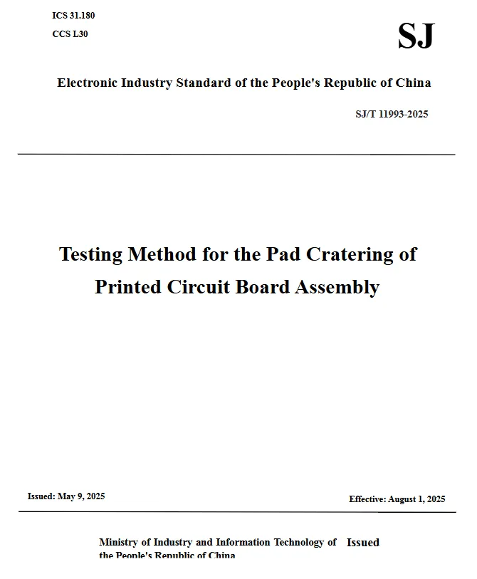
Testing Method for the Pad Cratering of Printed Circuit Board Assembly
Standard Details
SJ/T 11993-2025 (English Version)
- English translated version
- Sent to your email in 24h
SJ/T 11993-2025 (Chinese Version)
- Chinese original version
- Sent to your email in 12h
Standard Introduction
This standard provides a practical pull-pin solder-ball test method to assess the mechanical strength of PCB pads against cratering failure.
It covers the full workflow from sample preparation, solder paste placement, pull-pin alignment and solder ball formation, to reflow joint creation and vertical pull-off testing.
Four failure modes are defined: solder body cracking, solder interface fracture, pad peeling and pad cratering, along with the calculation method for pad strength based on maximum pull force and pad area.
Standard Catalog
The standard consists of the following main sections:
1 Scope 1
2 Normative References 1
3 Terms and Definitions 1
4 Test Principle 2
5 Test Environment 2
6 Test Apparatus 2
6.1 Pull-Pin 2
6.2 Solder Paste 3
6.3 Solder Placement Board 3
6.4 Stencil 3
6.5 Test Equipment 3
7 Test Procedure 4
7.1 Sample Preparation 4
7.2 Pre-placing Solder Paste Points 4
7.3 Pull-Pin Alignment with Solder Paste Point 4
7.4 Pull-Pin Insertion into Solder Paste Point 4
7.5 Heating Pull-Pin and Forming Solder Ball 5
7.6 Contacting Solder Ball with Pad 5
7.7 Heating Solder Ball to Form Solder Joint 5
7.8 Pulling the Pad 6
8 Result Expression 6
8.1 Failure Mode Description 6
8.2 Maximum Pad Pull Force 7
8.3 Pad Strength 7
9 Test Report 8
Appendix A (Informative) Pad Cratering Test Result Sample 9
English Version Preview
Preview coming soon. Need a sample? Contact us now.
Chinese Version Preview
Preview of the original Chinese version: