
SJ/T 11856.4-2025 Semiconductor Laser Chip Part 4: DBR Tunable Light Source Chip
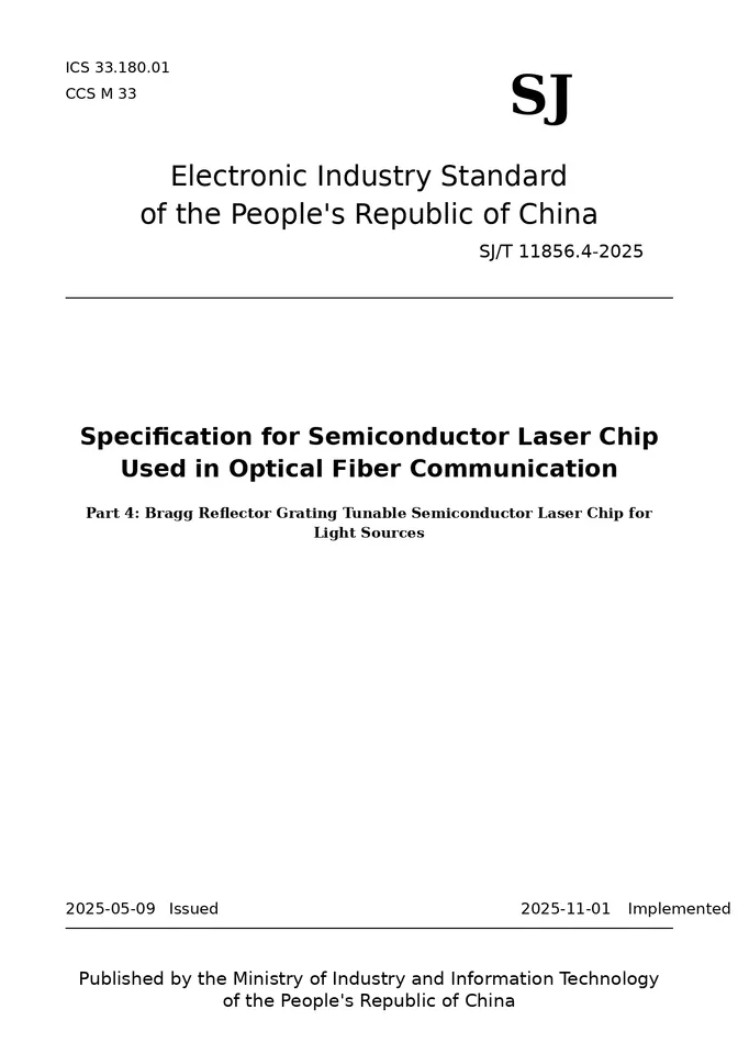
Specification for Semiconductor Laser Chip Used in Optical Fiber Communication - Part 4: Bragg Reflector Grating Tunable Semiconductor Laser Chip for Light Sources
Standard Details
SJ/T 11856.4-2025 (English Version)
- English translated version
- Sent to your email in 24h
SJ/T 11856.4-2025 (Chinese Version)
- Chinese original version
- Sent to your email in 12h
Standard Introduction
SJ/T 11856.4-2025 specifies the technical requirements for Bragg reflector grating tunable semiconductor laser chips used as light sources in optical fiber communication.
It covers terminology and definitions, abbreviations, optoelectronic characteristics, chip material, chip dimensions, surface quality, electrostatic discharge sensitivity, gold-wire bonding strength, shear force, environmental reliability, test methods, inspection rules, packaging and storage.
Standard Catalog
The standard consists of the following main sections:
1 Scope 1
2 Normative References 1
3 Abbreviations, Symbols and Definitions 1
3.1 Abbreviations 1
3.2 Symbols 1
3.3 Definitions 1
4 Classification 2
5 Requirements 2
5.1 Absolute Maximum Ratings 2
5.2 Optoelectronic Characteristics 2
5.2.1 DBR Chip Optoelectronic Characteristics 2
5.2.2 EML Chip Optoelectronic Characteristics 3
5.3 Chip Material 4
5.4 Chip Dimensions 4
5.5 Surface Quality 4
5.6 ESDS 4
5.7 Gold-Wire Bonding Strength 4
5.8 Shear Force 4
5.9 High-Temperature Storage 4
5.10 Low-Temperature Storage 4
5.11 Temperature Cycling 4
5.12 Steady Damp Heat 4
5.13 High-Temperature Life 4
6 Inspection Rules 5
6.1 Inspection Classification 5
6.2 Composition of Inspection Lots 5
6.3 Quality Assessment Procedure 5
6.4 Screening 5
6.5 Qualification Inspection 6
6.6 Quality Conformance Inspection 7
7 Test Methods 8
7.1 Test Environmental Conditions 8
7.2 Test Instruments and Equipment 8
7.3 Optoelectronic Characteristics 8
7.3.1 Threshold Current 8
7.3.2 Forward Optical Power 8
7.3.3 Extinction Ratio 9
7.3.4 Modulation Bandwidth 9
7.3.5 Forward Gain Voltage 10
7.3.6 Forward Modulation Voltage 10
7.3.7 -20 dB Spectral Width 10
7.3.8 Channel Spacing 10
7.3.9 Side-Mode Suppression Ratio 11
7.3.10 Slope Efficiency 11
7.3.11 Wavelength Temperature Drift Coefficient 11
7.3.12 Relative Intensity Noise 11
7.3.13 Vertical Far-Field Angle 12
7.3.14 Horizontal Far-Field Angle 12
7.4 Chip Dimensions 12
7.5 Surface Quality 12
7.6 Environmental Adaptability 12
7.6.1 ESDS 12
7.6.2 Gold-Wire Bonding Strength 12
7.6.3 Shear Force 12
7.6.4 High-Temperature Storage 12
7.6.5 Low-Temperature Storage 12
7.6.6 Temperature Cycling 12
7.6.7 Steady Damp Heat 12
7.6.8 High-Temperature Life 12
8 Packaging and Storage 13
8.1 Packaging 13
8.1.1 Product and Packaging Marking 13
8.1.2 Product Instructions 13
8.2 Storage 13
9 Precautions 13
Appendix A Wavelength Allocation Tables (Normative) 14
A.1 DWDM (100 GHz) Wavelength Allocation 14
A.2 DWDM (50 GHz) Wavelength Allocation 14
English Version Preview
Preview coming soon. Need a sample? Contact us now.
Chinese Version Preview
Preview of the original Chinese version: